Tel: +86-731-83521833        Mobile: +86 13574841950         info@chenguangjd.cn

big size Semiconductor Polycrystalline Cvd Diamond Wafer Polycrystalline thermally conductive cvd diamond film
Home » Products » Polycrystalline CVD Diamond » big size Semiconductor Polycrystalline Cvd Diamond Wafer Polycrystalline thermally conductive cvd diamond film

Product Category

Latest Products

" CVD / MCD technologies,  (111)-oriented diamond wire dies deliver unmatched precision for industrial wires, jewelry . And it have very long lifespan. "
0
0
Single Crystal HPHT Synthetic Diamond Plate for Cutting Tools
Size: 1-7mm
Thickness: 0.2-3mm
Shape: as you customize
0
0
Single crystal diamond CVD (chemical vapor deposition) refers to a type of diamond that is produced using the CVD process. In this process, a mixture of carbon-containing gases is decomposed under controlled conditions, resulting in the formation of a single crystal diamond layer on a substrate.

Single crystal diamond CVD is known for its exceptional hardness and thermal conductivity, which makes it useful for a range of industrial and scientific applications, such as cutting and grinding tools, heat spreaders, and optical components.

Compared to other forms of synthetic diamond, single crystal diamond CVD has a highly ordered crystal structure, which gives it improved physical and mechanical properties. This makes it a desirable material for a range of high-performance applications, where its hardness and thermal conductivity are important factors.

In summary, single crystal diamond CVD is a type of synthetic diamond that is produced using the CVD process and is characterized by its exceptional hardness and thermal conductivity. It has a wide range of applications in industries such as manufacturing, electronics, and optics.
 
 
0
0
Single crystal diamond CVD (chemical vapor deposition) refers to a type of diamond that is produced using the CVD process.

Single crystal diamond CVD is known for its exceptional hardness and thermal conductivity, which makes it useful for a range of industrial and scientific applications, such as cutting and grinding tools, heat spreaders, and optical components.

Compared to other forms of synthetic diamond, single crystal diamond CVD has a highly ordered crystal structure, which gives it improved physical and mechanical properties. This makes it a desirable material for a range of high-performance applications, where its hardness and thermal conductivity are important factors.
 
0
0
Diamond Semiconductor | Diamond Wafers | Diamond heat spreader
0
0
Synthetic diamond
The large size diamond crystal is an unprocessed diamond single crystal, which is made by high temperature and high pressure method. The size that our company can provide is generally 1mm -5mm large size single crystal with excellent performance, high hardness, good wear resistance, good corrosion resistance and high chemical stability, meeting various finishing tools (including single point, sheet, rotary and roller dresser, etc.), special cutting The application requirements of tools and indenters can also be used in the application of jewelry, crafts and other applications.
0
0

big size Semiconductor Polycrystalline Cvd Diamond Wafer Polycrystalline thermally conductive cvd diamond film

Diamond film refers to a diamond film artificially synthesized by low-pressure or atmospheric pressure chemical vapor deposition (CVD) method. There are two main methods for preparing diamond films: thermal chemical vapor deposition (TCVD) and plasma chemical vapor deposition (PCVD).
 
Size:
Orientation:
Availability:
Quantity:
facebook sharing button
twitter sharing button
line sharing button
wechat sharing button
linkedin sharing button
pinterest sharing button
sharethis sharing button
  • JSD

  • INFI

untra-thin CVD diamond film for  thermal conductivity 49*60*0.96

45mm cvd diamond wafer thermal Grade Polycrystalline CVD diamond for heat thread 

Specifications


1.High wear resistance to chipping and fracture
2.Excellent thermal stability
3.Excellent toughness sharpness
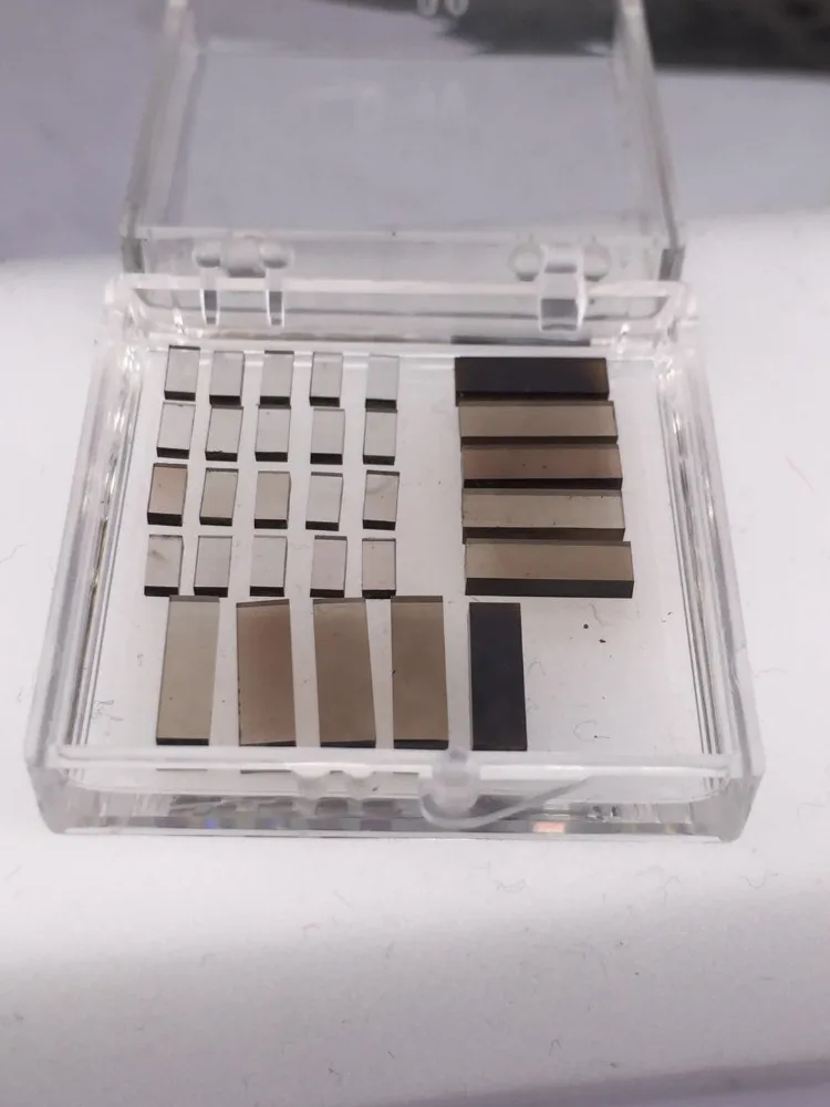
4.Various size


Polycrystalline CVD diamond


polycrystalline CVD (chemical vapour deposition) synthetic diamond products are manufactured by a chemical vapour deposition (CVD) process and are subject to tightly controlled growth conditions during manufacturing and equally stringent quality control procedures.


CVD Diamond for thermal applications:
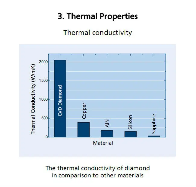
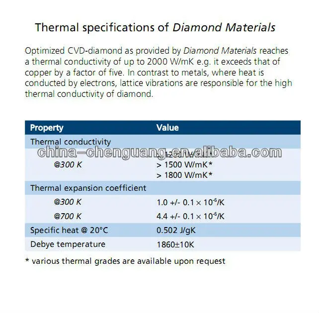
One of many remarkable properties of diamond is its unsurpassed thermal conductivity. It exceeds that of copper by a factor of five. In contrast to metals, where heat is conducted by electrons, lattice vibrations are responsible for the high thermal conductivity of diamond.   
 
Thermal conductivity can be tailored within the range of 1000-1800 W/mK to enable matching cost/performance to the needs of the application.
Nowadays CVD diamond made by our Laboratory is used as  mounts for high-power integrated circuits and laser diodes.
 
Specifications
  Tolerance of Thickness: ±25um
 Flatness: <4um/cm
 Thermal conductivity three types : 1300W/mK; 1500W/mK;1800 W/mK (more than 9 times compard to Silicone 139 W/mK)
 Density: 3.5g/cm3
 Young's modulus: 1000-1100Gpa
 Growth side surface finish: <100 nm Ra
 Nucleation side surface finish: <30 nm Ra 

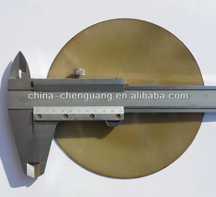
  Standard Sizes
  Size: Up to diameter 65 mm, larger sizes on request
 Surface: Both sides polished
 Raw thickness: Between 0.3 mm and 1.5 mm
 Polished thickness: Between 0.2 mm and 1.0 mm


_20180301135106


Previous: 
Next: 
HAVE A QUESTION?
CONTACT US NOW
We are always happy to answer all your questions.

Social Links

Diamonds Category

About Us

Contact Us
Office Address: Yuhua District,
Changsha City, Hunan Province, China
Factory address: Yanling,
Zhuzhou City,Hunan Province, China
Tel: +86-731-83521833 / +86-731-83521533
Copyright © 2021 INFI ADVANCED MATERIALS CO.,LTD      Sitemap      Technology By Leadong