 EnglishEnglish


| Quantity: | |
|---|---|


size 1-26mm
INFI
Boron-Doped Diamond (BDD) Electrode for Wastewater Treatment and Water Purification
Product Overview
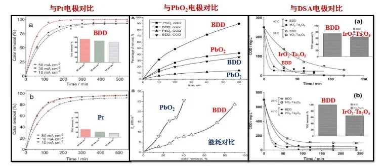
Boron-doped diamond (BDD) electrodes are used as anode components in wastewater treatment and water purification applications.
The BDD film is deposited on different substrate materials according to the required electrode structure. Available substrate options include monocrystalline silicon, polycrystalline silicon and niobium plate.
The electrode can be supplied in different shapes, including rectangular, square, mesh and disk forms. Custom shapes can also be reviewed according to the application and technical drawing.
General Characteristics
Product type: Boron-doped diamond (BDD) electrode
Main use: Wastewater treatment and water purification
Substrate options: Monocrystalline silicon, polycrystalline silicon or niobium plate
Electrode shapes: Rectangular, square, mesh, disk and custom shapes
Deposition method: Hot filament chemical vapor deposition (HFCVD)
Crystal type: Polycrystalline
Film structure: Microcrystalline
Film thickness: 10–20 μm
Edge treatment: Laser cut
Electrochemical Characteristics
The product description includes verified electrochemical data for the BDD film and electrode structure.
The electrochemical specification should be checked together with the following information:
Boron concentration
Film resistivity
Bulk resistivity
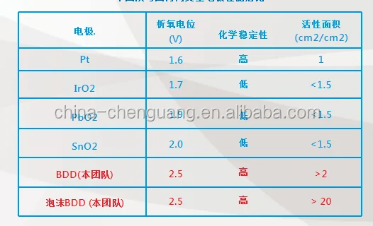
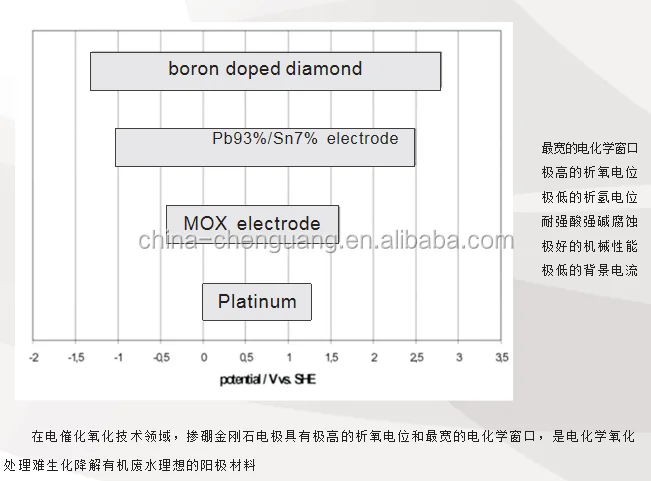
Potential window
Oxygen evolution potential
Hydrogen evolution potential
Measured potential range
The applicable values depend on the substrate, film structure and confirmed product specification. Please refer to the verified technical data for the final values and units.
Substrate Options
Monocrystalline Silicon Substrate
Monocrystalline silicon can be used as the substrate for BDD electrode deposition. It is suitable for electrode structures that require a silicon-based substrate.
Polycrystalline Silicon Substrate
Polycrystalline silicon can also be used as the substrate for BDD film deposition. The suitable size and structure should be confirmed according to the required application.
Niobium Plate Substrate
Niobium plate is available as a substrate option for BDD electrode production. It can be supplied in the required electrode shape and size according to the confirmed specification.
Available Electrode Shapes
The BDD electrode can be supplied in the following forms:
Rectangular electrode
Square electrode
Mesh electrode
Disk electrode
Custom-shaped electrode
The suitable shape depends on the water treatment equipment, installation method and required electrode area.
| No. | Product Name | Substrates | Specs | Unit |
| 1 | BDD Electrode | Silicon, single side coated | 5*5*0.55mm | Piece |
| 2 | BDD Electrode | Silicon, double side coated | 5*5*1.0mm 2 holes open | Piece |
| 3 | BDD Electrode | Silicon, double side coated | 5*5*1.0mm 4 holes open | Piece |
| 4 | BDD Electrode | Silicon, double side coated | 8*6*1 Slotting | Piece |
| 5 | BDD Electrode | Silicon, double side coated | 7*7*0.5mm | Piece |
| 6 | BDD Electrode | Silicon, single side coated | 10*10*0.625mm | Piece |
| 7 | BDD Electrode | Silicon, double side coated | 10*10*0.625mm | Piece |
| 8 | BDD Electrode | Silicon, double side coated | 10*10*0.5mm | Piece |
Applications
BDD electrodes are used in the following application areas:
Industrial wastewater treatment
Organic wastewater treatment
Water purification equipment
Electrochemical oxidation systems
Laboratory water treatment systems
Customized water treatment equipment
The exact electrode form and substrate should be selected according to the water composition, equipment structure and treatment requirements.
Product Size and Customization
Custom production can be reviewed according to the technical drawing.
Please provide the following information:
Substrate material
Electrode shape
Length and width
Diameter, if a disk electrode is required
Film thickness
Electrode quantity
Edge treatment
Installation method
Intended application
The final size and product structure should be confirmed before production.
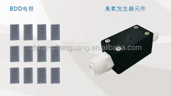
BDD Electrode Structure
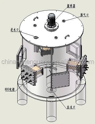
The BDD electrode consists of a diamond film deposited on the selected substrate.
The final electrode performance is related to:
Substrate material
BDD film structure
Boron concentration
Film thickness
Film resistivity
Electrode shape
Electrode size
Installation and operating conditions
Please confirm the required technical information before production so that the suitable electrode structure can be reviewed.
Water Treatment Application
BDD electrodes can be used in water treatment systems where an electrochemical oxidation electrode is required.
The actual treatment result depends on:
Wastewater composition
Organic matter concentration
Conductivity
Electrode area
Electrode spacing
Current and voltage conditions
Treatment time
Equipment structure
Operating conditions
The electrode should be selected together with the complete treatment system. The suitable product specification should be confirmed according to the actual water treatment application.
Frequently Asked Questions
Q1: What is a BDD electrode?
A BDD electrode is an electrode with a boron-doped diamond film deposited on a selected substrate. It is used in electrochemical water treatment and water purification applications.
Q2: Which substrates are available?
The current product specification includes monocrystalline silicon, polycrystalline silicon and niobium plate substrates.
Q3: What shapes are available?
Rectangular, square, mesh and disk shapes are available. Custom shapes can also be reviewed according to the technical drawing.
Q4: What is the BDD film thickness?
The current product specification lists a film thickness of 10–20 μm.


