 EnglishEnglish


| Size: | |
|---|---|
| Orientation: | |
| Quantity: | |


JSD
INFI
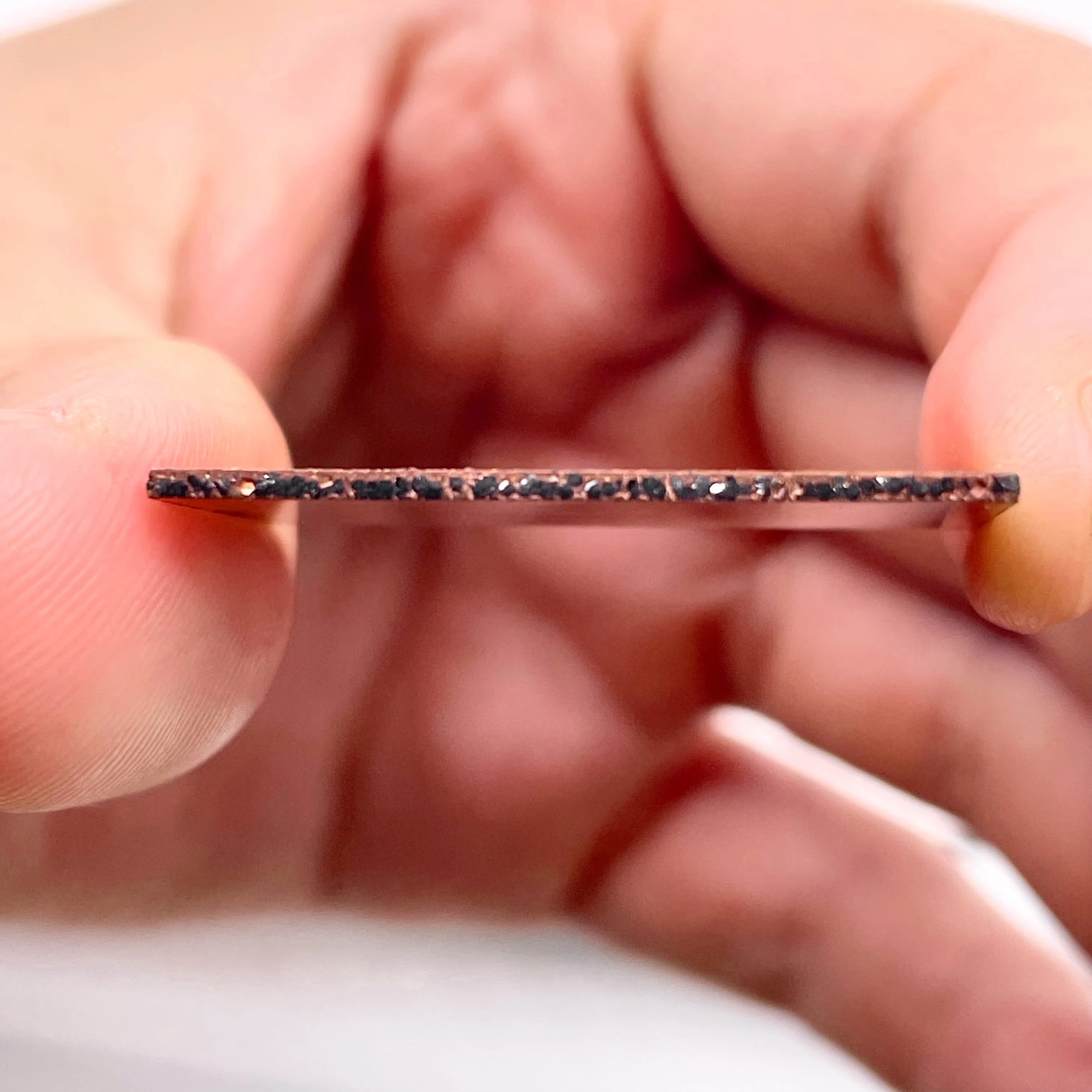
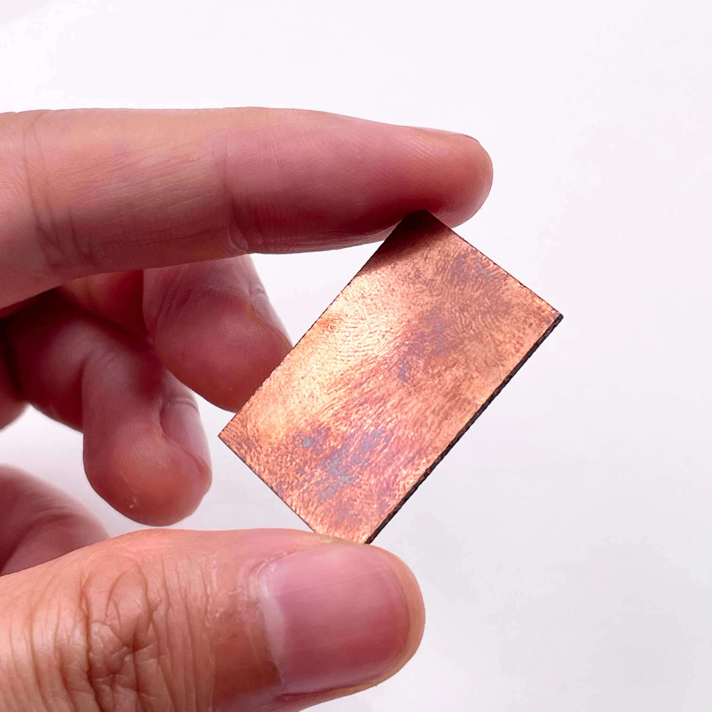
Copper Infiltrated Diamond Metal Matrix Composite (Cu-Diamond) for Semiconductor Laser / LED
Product Overview
Ultra-High Thermal Conductivity
Achieves 600–950 W/(m·K) – 1.5 to 2.5 times higher than pure copper (400 W/(m·K)).
Tailored CTE (Coefficient of Thermal Expansion)
Tunable from 5 to 10×10-6/K, precisely matching GaN, SiC, and Si chips. This minimizes thermal stress and improves long-term reliability.
Low Density & Lightweight
Density 5.0–7.0 g/cm³ – about 40% lighter than conventional W-Cu alloys.
Good Mechanical Strength
Bending strength > 278 MPa, excellent thermal cycling stability (performance drop <1% after 100 cycles).
Surface Metalization Compatible
Ready for direct bonding or soldering onto chips and heat sinks.
| Parameter | Value Range |
|---|---|
| Thermal Conductivity | 600 – 950 W/(m·K) (customizable up to 1000+) |
| CTE (25–200°C) | 5 – 10 ×10-6/K (adjustable by diamond volume fraction) |
| Density | 5.0 – 7.0 g/cm³ |
| Bending Strength | > 278 MPa |
| Diamond Volume Fraction | 40% – 70% |
| Surface Roughness (Ra) | ≤ 0.1 μm (polished) |
| Standard Thickness | 0.3 – 5.0 mm (custom available) |
| Max. Size | Up to 100×100 mm or custom shape |
AI & High-Performance Computing
Heat spreader for GPUs, AI accelerators, CPUs – reduces hotspot temperature by 10–20℃.
Power Electronics
Substrate or heat sink for IGBT, MOSFET, SiC power modules in EV (electric vehicles) and high-speed rail.
5G / RF Communication
Thermal management for RF power amplifiers in 5G base stations and phased array radar.
High-Power Lasers
Heat sink for laser diodes and fiber laser systems – CTE matches laser chip for stable output.
Aerospace & Defense
Lightweight, high-thermal-conductivity packaging for satellites, avionics, and missile electronics.
We use powder pressing + high-temperature sintering with advanced interface modification. Diamond particles are pre-coated with carbide-forming elements (Cr, Ti, W) to ensure strong bonding with copper matrix. This key step raises thermal conductivity from ~127 W/(m·K) (untreated) to over 600 W/(m·K).
Customizable: CTE, size, thickness, and diamond volume fraction tailored to your chip design.
Cost-Effective: Mass production capability with competitive pricing.
Quality Assurance: 100% inspection of thermal conductivity, CTE, and density before shipment.
Fast Lead Time: Samples in 7–10 days, mass production in 3–4 weeks.
MOQ: 10 pieces (sample order accepted)
Sample Policy: Samples available – please contact for pricing
Customization: OEM & ODM – drawing or sample based
Lead Time: 10–20 working days after order confirmation
Picture details:


