 EnglishEnglish


| Quantity: | |
|---|---|


scd23 SCD13 scd22 scd11
Infi
SCD diamond
HPHT Wafers/Substrates
1. Primary Applications:
Quantum Technologies: As substrates for Nitrogen-Vacancy (NV) centers and other color centers, used in quantum sensors, magnetometers, and quantum information processing chips.
High-Power Electronics: As heat spreaders or direct substrates for fabricating high-voltage, high-frequency diamond-based transistors (FETs) for RF and power conversion systems.
Thermal Management: As highly efficient thermal interface materials (TIMs) or heat sinks for high-performance computing (HPC), laser diodes, and power amplifiers.
Optics & Windows: For high-durability infrared (IR) and terahertz (THz) windows, lenses, and optical components in harsh environments (e.g., aerospace, spectroscopy).
High-Pressure Research: As anvils in Diamond Anvil Cells (DACs) to generate extreme pressures for material science and geophysics research.
Surface Acoustic Wave (SAW) Devices: As piezoelectric substrates for high-frequency, low-loss SAW filters and sensors.
Biomedical & Electrochemical Sensors: As electrodes or functionalized surfaces for biosensing and electrochemical detection due to diamond's biocompatibility and wide electrochemical window.
Semiconductor Substrates: For the heteroepitaxial growth of other wide-bandgap materials (e.g., GaN) to improve thermal performance.
2. Key Advantages (Specific to Round HPHT Single-Crystal Diamond):Superior Material Quality: HPHT synthesis produces high-purity, Type IIa diamond with exceptionally low nitrogen and defect concentrations, leading to excellent optical transparency and electronic properties.
High Crystalline Perfection: Single-crystal HPHT diamond has minimal grain boundaries and dislocations, which is critical for high-performance electronic and quantum applications.
Extreme Thermal Conductivity: The highest known thermal conductivity (~2200 W/m·K) enables unparalleled heat dissipation.
Round Form Factor: A round (wafer) shape is ideal and standard for many fabrication processes:
Compatible with standard semiconductor wafer-handling tools (chucks, cassettes).
Suitable for photolithography, thin-film deposition, and dicing processes commonly used in semiconductor and optics industries.
Enables efficient patterning and device integration across the surface.
Controlled Doping & Functionalization: HPHT diamonds can be doped during growth (e.g., with boron for p-type conductivity) or have their surfaces functionalized for specific applications.
Exceptional Mechanical & Chemical Properties: Extreme hardness, wear resistance, and chemical inertness ensure long-term reliability in demanding environments.
Comparison Context:
vs. CVD Single-Crystal Diamond: HPHT wafers often offer higher crystalline perfection for a given size, but size is limited by the press chamber. CVD is better for scaling up to larger area wafers.
vs. Polycrystalline Diamond (PCD): Single-crystal HPHT is superior for electronic, quantum, and optical applications where grain boundaries are detrimental. PCD is more cost-effective for large-area wear parts and some thermal applications.
Size Available:
| Size: | |
|---|---|
| Thickness: | |
| Grade: | |
| Model No. | Picture | Feature | Size range | Available thickness | Shape | Orientation |
| JSD11 |    | Laser cut to specific dimension and standard rectangles, triangles, circles, trapezoidsand other required shapes according to customer requirements. | 0.3mm~ 5.0mm | 0.3mm ~ 1.7 mm | Rectangle, triangle, circle and others | 4 pt / (100) |
| JSD12 |  | Yellow color, At least two 90° angles, The other two corners are two very small missing corners. More regular shape, suitable for ultra-precision machining of diamond with long cutting edge, Under the microscope there are few impurities and no microcracks. | 1mm ~ 4.5mm | 0.3mm ~ 1.7 mm | Near Square | 4 pt / (100) |
| JSD13 | 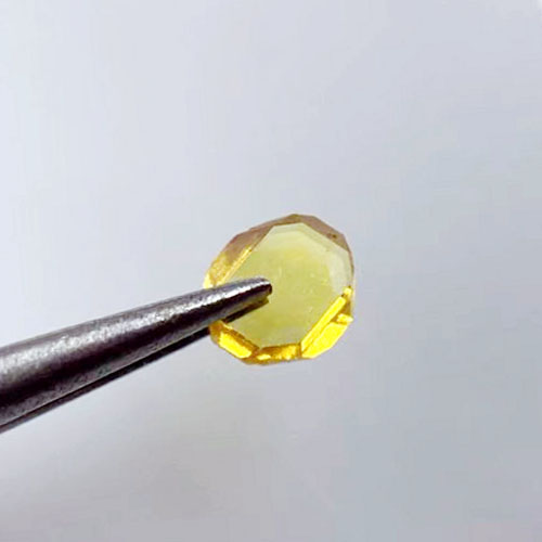 | Pale yellow color, Irregular shape, Under the microscope there are few impurities and no microcracks. The maximum size can reach 8 mm and the maximum thickness can reach 1.7 mm, | 1mm ~ 8.0 mm | 0.3mm ~ 1.7 mm | Near hexagon | 4 pt / (100) |
| JSD23 | 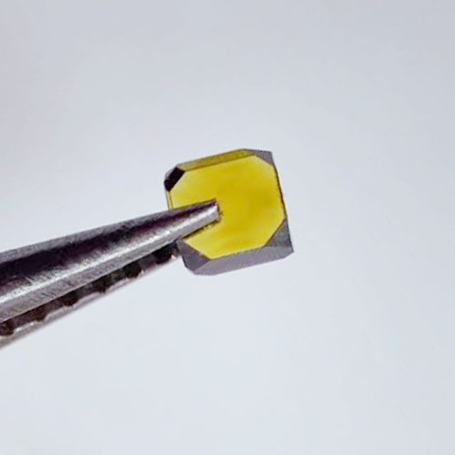 | Yellow color, Near Square, four very small missing corners. some pieces have slightly visible impurites, The maximum size can reach 8 mm and the maximum thickness can reach 1.7 mm, | 1mm ~ 8.0 mm | 0.3mm ~ 1.7 mm | Near Square | 4 pt / (100) |
| JSD33 | 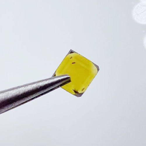 | Irregular shape, with a few visible impurites or growth grooves. Suitable for low-end diamond tools. | 1mm ~ 8.0 mm | 1.0mm ~1.2mm | Near Square | 4 pt / (100) |
| JSD111 |  | with strong wear resistance, We guarantee that there is a certain implied circle and there are no impurities in the crystal. Used for wire drawing die blanks | 0.8mm-3.5mm | 0.3mm-2.0mm | Near hexagon or near triangle | 3pt /( 111) |
HPHT Diamond Plate
Product Details Specification:
1. Best surface finish of any die material available.
2. Moth’s hardness 10
3. Good thermal stability
4.Good shock resistance
Main Application:
1. For fine wire and ultrafine wire applications demanding a superior wire surface finish, nothing performs better than a single crystal natural or synthetic diamond die.
2. Used in Diamond cutting tools, LED polishing, jewelry cutting and carving, correct pen,flywheel, Diamond wheel dressing tools and so on
3. For all kinds of geological exploration drilling tools, engineering drilling tools, and all varieties of diamond drilling tools
4. High purity, toughness and good thermal stability
5. Physical appearance of our diamond plate is no black spot, no crake, and good sharp


