 EnglishEnglish


| Quantity: | |
|---|---|


JSD
Infi
MCD ,Advantages of the <111> Orientation in Single-Crystal Diamond
The <111> direction, corresponding to the {111} crystal planes, is one of the most significant and technologically valuable orientations in diamond due to its unique structural and property extremes.
1. Highest Hardness and Wear Resistance
The {111} planes have the highest atomic planar density in the diamond cubic lattice. Cutting or abrading along this direction requires breaking the maximum number of strong covalent C-C bonds per unit area, resulting in the ultimate hardness and wear resistance of any crystal orientation. This makes it preferred for ultra-durable cutting tools and wear-resistant coatings.
2. Exceptional Thermal Conductivity
Diamond's thermal conductivity is anisotropic. The <111> direction typically exhibits the highest thermal conductivity (exceeding 2200 W/m·K at room temperature). This makes it the optimal choice for thermal management solutions, such as heat spreaders and sinks in high-power density electronic and photonic devices.
3. Superior Chemical and Thermal Stability
The dense, stable termination of the {111} surface confers enhanced chemical inertness and thermal stability compared to other orientations (like {100}). It is more resistant to graphitization at high temperatures in non-inert atmospheres and less reactive in harsh chemical environments.
4. Preferred Orientation for High-Quality Homoepitaxy and Doping
The {111} plane is the slowest-growing and most stable facet under standard CVD growth conditions. It is the preferred substrate for homoepitaxial growth of high-purity, low-defect single-crystal diamond layers.
Certain impurity atoms, particularly nitrogen, incorporate more readily into the {111} growth sector. This allows for more controlled and efficient doping, which is crucial for creating specific color centers like the Nitrogen-Vacancy (NV) center for quantum sensing and information applications.
5. Ideal for Quantum Technologies (NV Center Formation)
The controlled incorporation of nitrogen and the subsequent creation of NV- centers are most effective on {111}. A key advantage is that the NV axis is aligned with the <111> crystal direction. This provides a well-defined quantization axis and simplifies device design and spin readout in quantum systems.
6. Surface Functionalizability
The {111} surface can be terminated with hydrogen, oxygen, or fluorine to create well-defined and stable surface chemistries. This ease of functionalization is vital for attaching biomolecules for sensing, creating low-friction surfaces, or facilitating electronic device fabrication.
7. Suitability for High-Pressure Research
Due to its extreme hardness and strength, <111>-oriented diamond anvils are used in Diamond Anvil Cells (DACs) for ultra-high-pressure experiments, where maximum resistance to deformation is required.
Summary of Key Applications:
Ultra-Hard Tools & Coatings: Cutting, drilling, and grinding tools.
Thermal Management: Heat spreaders for high-power lasers, RF devices, and CPUs.
Quantum Technologies: Substrates for NV-center-based sensors, magnetometers, and quantum processors.
Electronics: Potential substrates for high-voltage, high-frequency diamond semiconductors.
High-Pressure Physics: Anvils in Diamond Anvil Cells (DACs).
Biomedical & Sensors: Functionalized surfaces for electrochemical electrodes and bio-sensors.
Optics: High-durability infrared windows and lenses.
In essence, the <111> orientation leverages diamond's most extreme intrinsic properties—maximum hardness, thermal conductivity, and stability—making it the premier choice for the most demanding scientific and industrial applications.
Size Available:
Size: | 2x2mm 2.5x2.5mm 3.0x3.0mm 3.5x3.5mm 4.0x4.0mm 4.5x4.5mm 5.0x5.0mm 5.5x5.5mm 6.0x6.0mm 6.5x6.5mm 7.0x7.0mm 7.5x7.5mm | Thickness: | 0.3mm 0.5mm 0.8mm 1.0mm 1.5mm Csutomized | Grade: | JSD11 JSD12 JSD23 JSD13 JSD33 JSD111 |
| Model No. | Picture | Feature | Size range | Available thickness | Shape | Orientation |
| JSD11 |    | Laser cut to specific dimension and standard rectangles, triangles, circles, trapezoidsand other required shapes according to customer requirements. | 0.3mm~ 5.0mm | 0.3mm ~ 1.7 mm | Rectangle, triangle, circle and others | 4 pt / (100) |
| JSD12 |  | Yellow color, At least two 90° angles, The other two corners are two very small missing corners. More regular shape, suitable for ultra-precision machining of diamond with long cutting edge, Under the microscope there are few impurities and no microcracks. | 1mm ~ 4.5mm | 0.3mm ~ 1.7 mm | Near Square | 4 pt / (100) |
| JSD13 | 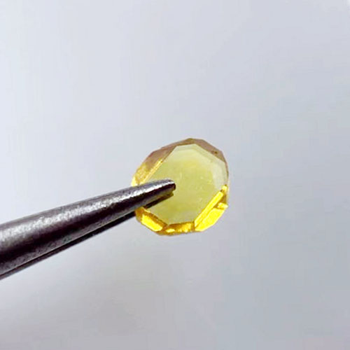 | Pale yellow color, Irregular shape, Under the microscope there are few impurities and no microcracks. The maximum size can reach 8 mm and the maximum thickness can reach 1.7 mm, | 1mm ~ 8.0 mm | 0.3mm ~ 1.7 mm | Near hexagon | 4 pt / (100) |
| JSD23 | 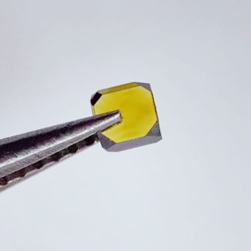 | Yellow color, Near Square, four very small missing corners. some pieces have slightly visible impurites, The maximum size can reach 8 mm and the maximum thickness can reach 1.7 mm, | 1mm ~ 8.0 mm | 0.3mm ~ 1.7 mm | Near Square | 4 pt / (100) |
| JSD33 | 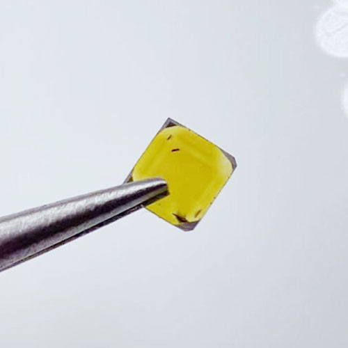 | Irregular shape, with a few visible impurites or growth grooves. Suitable for low-end diamond tools. | 1mm ~ 8.0 mm | 1.0mm ~1.2mm | Near Square | 4 pt / (100) |
| JSD111 |  | with strong wear resistance, We guarantee that there is a certain implied circle and there are no impurities in the crystal. Used for wire drawing die blanks | 0.8mm-3.5mm | 0.3mm-2.0mm | Near hexagon or near triangle | 3pt /( 111) |
HPHT Diamond Plate
Product Details Specification:
1. Best surface finish of any die material available.
2. Moth’s hardness 10
3. Good thermal stability
4.Good shock resistance
Main Application:
1. For fine wire and ultrafine wire applications demanding a superior wire surface finish, nothing performs better than a single crystal natural or synthetic diamond die.
2. Used in Diamond cutting tools, LED polishing, jewelry cutting and carving, correct pen,flywheel, Diamond wheel dressing tools and so on
3. For all kinds of geological exploration drilling tools, engineering drilling tools, and all varieties of diamond drilling tools
4. High purity, toughness and good thermal stability
5. Physical appearance of our diamond plate is no black spot, no crake, and good sharp


