 EnglishEnglish


| Quantity: | |
|---|---|


SCD23、SCD13、SCD22、SCD11
INFI
Industrial Applications
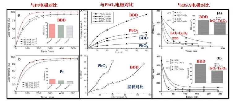
Boron-doped diamond (BDD) electrodes effectively treat complex wastewater streams, including:
Pharmaceutical/Chemical Processing Residues
Explosive Manufacturing Effluents
Textile Dye & Leather Tanning Waste
Petrochemical & Metallurgical Byproducts
Landfill Leachate & Distillery Discharge
| No. | Product Name | Substrates | Specs | Unit |
| 1 | BDD Electrode | Silicon, single side coated | 5*5*0.55mm | Piece |
| 2 | BDD Electrode | Silicon, double side coated | 5*5*1.0mm 2 holes open | Piece |
| 3 | BDD Electrode | Silicon, double side coated | 5*5*1.0mm 4 holes open | Piece |
| 4 | BDD Electrode | Silicon, double side coated | 8*6*1 Slotting | Piece |
| 5 | BDD Electrode | Silicon, double side coated | 7*7*0.5mm | Piece |
| 6 | BDD Electrode | Silicon, single side coated | 10*10*0.625mm | Piece |
| 7 | BDD Electrode | Silicon, double side coated | 10*10*0.625mm | Piece |
| 8 | BDD Electrode | Silicon, double side coated | 10*10*0.5mm | Piece |
Operational Superiority
Eco-Efficient Degradation: 40% faster organic breakdown vs. traditional PbO₂/Pt anodes
Chemical Resilience: Maintains integrity in acidic/alkaline environments
Ozone Synthesis: Generates ozone without electrolytes for sustainable purification
Material Science Excellence
Bandgap Advantage: 5.47 eV enables operation above 500°C
Thermal Mastery: 2,200 W/mK conductivity minimizes thermal resistance in laser systems
Electron Dynamics: Superior hole mobility for high-frequency RF circuits
Performance Benchmarks
Keyes Index: Optimal for microelectronic miniaturization
Johnson Index: 8,200 (20x GaN’s 280) for high-power amplifiers
Cold Cathode Capability: Achieved via negative electron affinity

Engineered Thermal Solutions
Custom Conductivity: 1,000–1,800 W/mK (adjustable for cost-performance balance)
Precision Fabrication:
Thickness Control: ±25 μm
Ultra-Flat Surfaces: <4 μm/cm deviation
Dual-Side Polishing: Growth face <100 nm Ra, nucleation face <30 nm Ra
Standard Offerings
Dimensions: Standard Ø65 mm (custom sizes available)
Thickness Options:
As-grown: 0.3–1.5 mm
Polished: 0.2–1.0 mm
Mechanical Metrics:
Density: 3.5 g/cm³
Stiffness: 1,000–1,100 GPa Young’s modulus
Critical Use Cases
Thermal spreaders for high-density IC packaging
Heat sinks in aerospace laser arrays
Compact cooling modules for 5G infrastructure


