Tel: +86-731-83521833        Mobile: +86 13574841950         info@chenguangjd.cn

Boron Doped Diamond CVD Diamond BDD Electrode for Waster Water Treatment Conductive Pure Water BDD
Home » Products » BDD » Boron Doped Diamond CVD Diamond BDD Electrode for Waster Water Treatment Conductive Pure Water BDD

Product Category

Latest Products

" CVD / MCD technologies,  (111)-oriented diamond wire dies deliver unmatched precision for industrial wires, jewelry . And it have very long lifespan. "
0
0
Single Crystal HPHT Synthetic Diamond Plate for Cutting Tools
Size: 1-7mm
Thickness: 0.2-3mm
Shape: as you customize
0
0
Single crystal diamond CVD (chemical vapor deposition) refers to a type of diamond that is produced using the CVD process. In this process, a mixture of carbon-containing gases is decomposed under controlled conditions, resulting in the formation of a single crystal diamond layer on a substrate.

Single crystal diamond CVD is known for its exceptional hardness and thermal conductivity, which makes it useful for a range of industrial and scientific applications, such as cutting and grinding tools, heat spreaders, and optical components.

Compared to other forms of synthetic diamond, single crystal diamond CVD has a highly ordered crystal structure, which gives it improved physical and mechanical properties. This makes it a desirable material for a range of high-performance applications, where its hardness and thermal conductivity are important factors.

In summary, single crystal diamond CVD is a type of synthetic diamond that is produced using the CVD process and is characterized by its exceptional hardness and thermal conductivity. It has a wide range of applications in industries such as manufacturing, electronics, and optics.
 
 
0
0
Single crystal diamond CVD (chemical vapor deposition) refers to a type of diamond that is produced using the CVD process.

Single crystal diamond CVD is known for its exceptional hardness and thermal conductivity, which makes it useful for a range of industrial and scientific applications, such as cutting and grinding tools, heat spreaders, and optical components.

Compared to other forms of synthetic diamond, single crystal diamond CVD has a highly ordered crystal structure, which gives it improved physical and mechanical properties. This makes it a desirable material for a range of high-performance applications, where its hardness and thermal conductivity are important factors.
 
0
0
Diamond Semiconductor | Diamond Wafers | Diamond heat spreader
0
0
Synthetic diamond
The large size diamond crystal is an unprocessed diamond single crystal, which is made by high temperature and high pressure method. The size that our company can provide is generally 1mm -5mm large size single crystal with excellent performance, high hardness, good wear resistance, good corrosion resistance and high chemical stability, meeting various finishing tools (including single point, sheet, rotary and roller dresser, etc.), special cutting The application requirements of tools and indenters can also be used in the application of jewelry, crafts and other applications.
0
0

Boron Doped Diamond CVD Diamond BDD Electrode for Waster Water Treatment Conductive Pure Water BDD

Boron doped diamond (BDD), also known as boron doped diamond, is a new type of electrode material prepared by doping boron elements into diamond films through techniques such as chemical vapor deposition (CVD). This material not only inherits many excellent properties of natural diamond, such as high hardness, high thermal conductivity, and chemical inertness, but also obtains good conductivity and semiconductor properties through boron doping. These unique properties have demonstrated enormous application potential for BDD in multiple high-tech fields.
Availability:
Quantity:
facebook sharing button
twitter sharing button
line sharing button
wechat sharing button
linkedin sharing button
pinterest sharing button
sharethis sharing button
  • scd23 SCD13 scd22 scd11

  • Infi

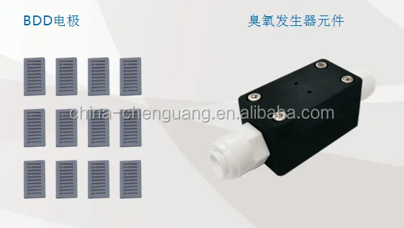
BDD electrode for waster water treatment and Water purifier production

Specifications

BDD electrodes can effectively degrade various organic waste water, such as organic waste water in the fields of medicine /agrochemicals, petrochemicals, coking, smelting, printing and dyeing,
papermaking, tanning, explosives, wine making, landfill leachate, etc.


No. Product Name Substrates Specs Unit
1 BDD Electrode Silicon, single side coated 5*5*0.55mm Piece
2 BDD Electrode Silicon, double side coated 5*5*1.0mm
2 holes open
Piece
3 BDD Electrode Silicon, double side coated 5*5*1.0mm
4 holes open
Piece
4 BDD Electrode Silicon, double side coated 8*6*1
Slotting
Piece
5 BDD Electrode Silicon, double side coated 7*7*0.5mm Piece
6 BDD Electrode Silicon, single side coated 10*10*0.625mm Piece
7 BDD Electrode Silicon, double side coated 10*10*0.625mm Piece
8 BDD Electrode Silicon, double side coated 10*10*0.5mm Piece

 Advangtages

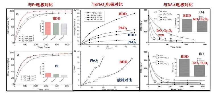
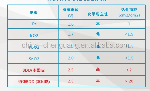
Under the same conditions, the efficiency and energy consumption of BDD electrodes in degrading organics are significantly better than other electrodes


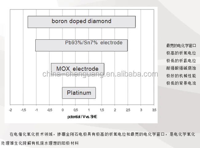
Although using P b O 2 plates or P t nets as anodes can effectively generate ozone, they have disadvantages such as low durability, high price, and harmful effects to the environment. Boron-doped diamond (B D D) electrodes have also been reported to produce ozone without the use of any electrolyte. The applications of B D D in extreme electrochemistry, such as wastewater treatment and the synthesis of hydroxyl and methoxy groups, have been well documented. Due to its excellent chemical and physical stability, B D D is used in ozone-generated anode materials.


CVD diamond BDD Application:

Pure CVD Polycrystalline BDD Diamond Electrode Membrane Pem Ozone GeneratorPure CVD Polycrystalline BDD Diamond Electrode Membrane Pem Ozone GeneratorPure CVD Polycrystalline BDD Diamond Electrode Membrane Pem Ozone GeneratorPure CVD Polycrystalline BDD Diamond Electrode Membrane Pem Ozone Generator


Firstly, BDD has an extremely high bandgap (about 5.47 eV), much higher than silicon (1.1 eV), silicon carbide (4H SiC, 3.2 eV), and gallium nitride (GaN, 3.44 eV). This characteristic makes it an ideal material for manufacturing high-temperature and high-frequency electronic devices. Secondly, BDD has the highest thermal conductivity among all known materials, which not only increases the operating temperature range of the device, but also significantly reduces the size and weight of the device, which is beneficial for manufacturing high-performance amplifiers and lasers.

In addition, BDD has the highest electron saturation rate under high electric fields, and its hole mobility is also the highest among all wide bandgap semiconductor materials. These characteristics make BDD particularly suitable for millimeter wave amplifiers and high-speed integrated circuits. At the same time, BDD also has excellent electron emission capability and can achieve negative electron affinity after special treatment, making it an ideal choice for making cold cathodes.

Not only that, BDD also performs well in key semiconductor performance indicators such as Johnson index, Keyes index, and Baliga index. For example, its Johnson index is as high as 8200, far exceeding 4H SiC (410) and GaN (280). This means that BDD has unparalleled advantages in power amplifiers, integrated circuits, and switching devices.

BDD has a wide range of applications, covering flat displays, microelectronics MEMS/NEMS、 Strong electricity and electrochemistry, among other aspects. Especially in electrochemical sensors, BDD has become an ideal material for the new generation of high-performance electrochemical sensors due to its high conductivity, wide potential window, low background current value, and excellent anti pollution ability.


Polycrystalline CVD diamond

polycrystalline CVD (chemical vapour deposition) synthetic diamond products are manufactured by a chemical vapour deposition (CVD) process and are subject to tightly controlled growth conditions during manufacturing and equally stringent quality control procedures.


CVD Diamond for thermal applications:
One of many remarkable properties of diamond is its unsurpassed thermal conductivity. It exceeds that of copper by a factor of five. In contrast to metals, where heat is conducted by electrons, lattice vibrations are responsible for the high thermal conductivity of diamond.   
 
Thermal conductivity can be tailored within the range of 1000-1800 W/mK to enable matching cost/performance to the needs of the application.
Nowadays CVD diamond made by our Laboratory is used as  mounts for high-power integrated circuits and laser diodes.
 
Specifications
  Tolerance of Thickness: ±25um
 Flatness: <4um/cm
 Thermal conductivity three types : 1300W/mK; 1500W/mK;1800 W/mK (more than 9 times compard to Silicone 139 W/mK)
 Density: 3.5g/cm3
 Young's modulus: 1000-1100Gpa
 Growth side surface finish: <100 nm Ra
 Nucleation side surface finish: <30 nm Ra 

  Standard Sizes
  Size: Up to diameter 65 mm, larger sizes on request
 Surface: Both sides polished
 Raw thickness: Between 0.3 mm and 1.5 mm
 Polished thickness: Between 0.2 mm and 1.0 mm


Previous: 
Next: 
HAVE A QUESTION?
CONTACT US NOW
We are always happy to answer all your questions.

Social Links

Diamonds Category

About Us

Contact Us
Office Address: Yuhua District,
Changsha City, Hunan Province, China
Factory address: Yanling,
Zhuzhou City,Hunan Province, China
Tel: +86-731-83521833 / +86-731-83521533
Copyright © 2021 INFI ADVANCED MATERIALS CO.,LTD      Sitemap      Technology By Leadong