EnglishEnglish
Views: 554


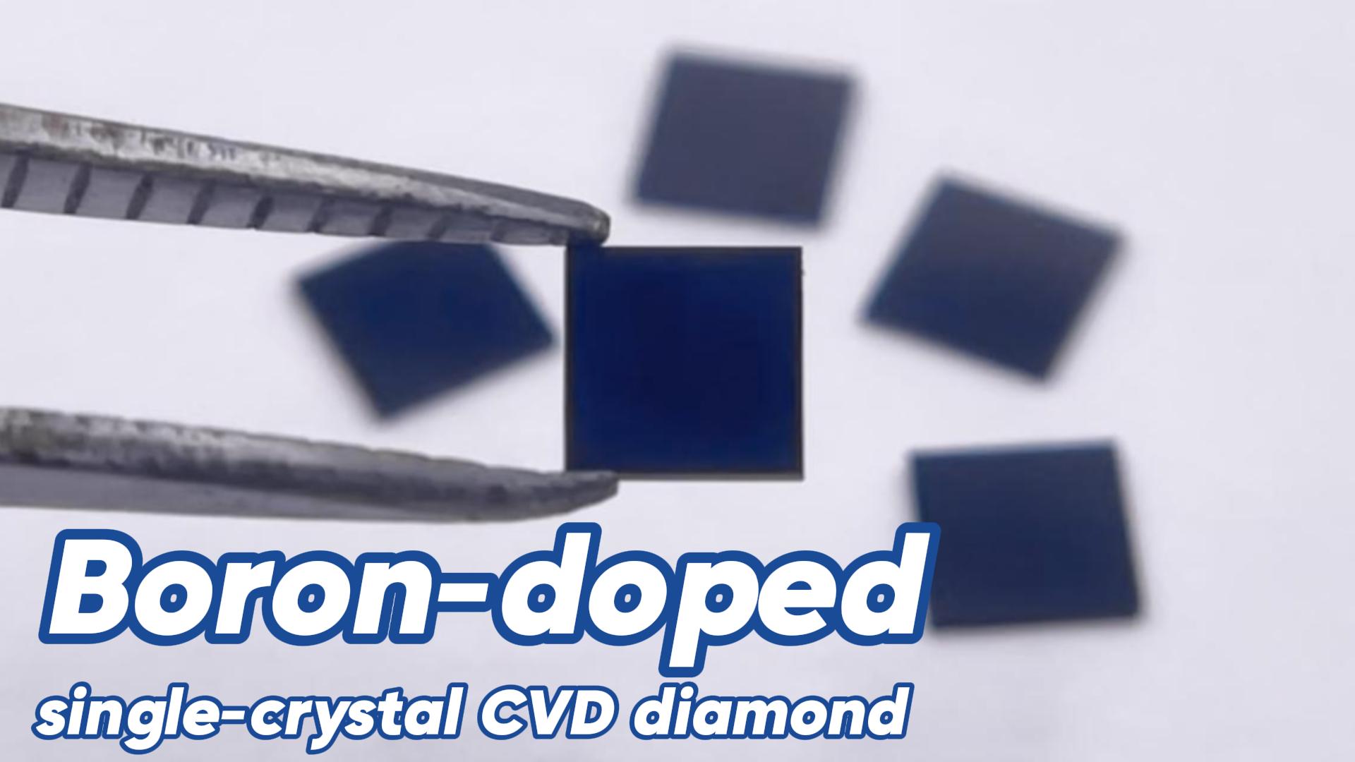
Boron Doped Diamond (BDD) represents one of the most sophisticated achievements in synthetic diamond technology. By intentionally introducing boron atoms into the diamond crystal lattice during chemical vapor deposition (CVD), this material transforms from an exceptional insulator into a powerful semiconductor while retaining all of diamond's legendary extreme properties.
The Science of Boron Doping
When boron atoms substitute for carbon atoms in the diamond lattice, they act as acceptor impurities, creating a shallow energy level approximately 0.37 eV above the valence band . This produces p-type semiconducting behavior, with hole carriers enabling electrical conduction. The doping concentration can be precisely controlled, allowing electrical resistivity to be tuned across a remarkable range—from highly insulating to metallic-like conductivity .
Recent advances in microwave plasma CVD (MPCVD) technology have enabled the growth of high-quality boron-doped single crystal diamond films with exceptional crystalline perfection. X-ray diffraction analysis shows peak full width at half maximum values below 60 arcseconds, indicating excellent crystal quality . Hall effect measurements demonstrate precise control over hole concentrations from 10¹⁴ to 10¹⁷ cm⁻³, with room-temperature hole mobility exceeding 1,400 cm²/(V·s)—reaching internationally advanced levels .
Electrical and Thermal Properties
The boron concentration fundamentally determines the material's behavior. At doping levels around 10¹⁸ cm⁻³, insulating diamond transforms to semiconducting diamond, while concentrations above 10²¹ cm⁻³ produce metallic conductivity . Highly doped BDD achieves electrical resistivity as low as 0.05 Ω·cm, making it suitable for demanding electronic applications .
However, heavy boron doping does influence thermal transport. Research shows that high boron concentrations (e.g., 10²⁰ cm⁻³) can reduce room-temperature thermal conductivity by approximately a factor of four compared to undoped diamond . While undoped diamond exhibits thermal conductivity proportional to 1/T between 300 and 800 K, boron-doped diamond displays a more complex behavior—thermal conductivity increases by about 20% between 300 and 500 K before decreasing above 500 K . This non-monotonic behavior suggests that boron suppresses phonon transport across both high and low frequencies through point defect scattering and hole-phonon interactions . Despite this reduction, heavily doped BDD still offers thermal conductivity around 700 W/m·K—far exceeding most engineering materials .
Advanced Applications
The unique combination of tunable conductivity and diamond's extreme properties positions BDD as an enabling material for cutting-edge technologies:
High-Power Electronics: As a wide bandgap semiconductor (~5.5 eV), diamond devices can operate at significantly higher voltages and temperatures than silicon-based alternatives. BDD enables diamond-based Schottky diodes, field-effect transistors, and high-voltage switches capable of reliable operation above 500°C in harsh environments such as aerospace, nuclear industry, and deep-well drilling applications.
RF and Microwave Devices: Electrically conductive BDD serves as an ideal heat spreader for RF/microwave devices. Mounting high-power amplifiers on BDD heat spreaders enables better isolation of the ground plane below 1.5 GHz and reduces conductive losses at higher frequencies due to increased skin depth . This makes BDD valuable for 5G infrastructure, satellite communications, and defense radar systems.
Thermal Management with Electrical Functionality: BDD uniquely combines high thermal conductivity with electrical conductivity, allowing it to function simultaneously as a heat spreader and an electrical interconnect or electrode . This replaces traditional multi-layer metal/diamond configurations, enabling more compact and efficient thermal management solutions for high-power laser diodes, RF amplifiers, and power modules.
Advanced Electrode Applications: The wide electrochemical window and low background current of BDD make it exceptional for electrochemical sensing, supercapacitor electrodes, and applications requiring stable, corrosion-resistant electrodes . Its chemical inertness ensures reliable performance even in aggressive environments.
Emerging Quantum Technologies: Boron-doped diamond is also finding applications in quantum sensing, where its acceptor nature can influence the charge state of nitrogen-vacancy centers for advanced quantum sensing applications .
Conclusion
Boron Doped Diamond represents a remarkable fusion of diamond's intrinsic extremes with engineered electronic functionality. Through precise control of boron incorporation during CVD growth, this material delivers tunable p-type conductivity while preserving unparalleled hardness, thermal conductivity, and chemical stability. As research continues to push the boundaries of crystalline quality and doping control, BDD stands poised to enable next-generation advances in high-power electronics, RF systems, thermal management, and quantum technologies.